Electrical
Maximum Ratings
Table 2. Electrical SpecificationsPARAMETER
VALUE
Operating Voltage : Nominal
+28.0 VDC
Maximum
+ 30 VDC
Minimum
+ 14.0 VDC
Power Consumption : Electronics (Maximum)
28 Watts @ +28 VDC
Power Consumption : Electronics (Nominal)
10 Watts @ +28 VDC
Pin Assignments J1
Figure 3. J1 - 22-Pin Connector Diagram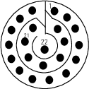 Table 3. Pin Assignments for J1
PIN
FUNCTION
TYPE
INPUT/OUTPUT
1
DC GND
Analog
Input
2
28VDC-IN
Analog
Input
3
CHASSIS
Analog
Input
4
RESERVED, NOT CONNECTED
5
PWM 1 POWER
Analog
Output
6
PWM 1 RTN
Analog
Output
7
ENTER-KEY-OUT
Discrete
Output
8
PWM 2 POWER
Analog
Output
9
PWM 2 RTN
Analog
Output
10
RESERVED, NOT CONNECTED
11
PWM 3 POWER
Analog
Output
12
PWM 3 RTN
Analog
Output
13
RESERVED, NOT CONNECTED
14
RESERVED, NOT CONNECTED
15
RESERVED, NOT CONNECTED
16
ARINC-429-IN-A
A429
Input
17
ARINC-429-IN-B
A429
Input
18
RESERVED, NOT CONNECTED
19
ARINC-429-OUT-A
A429
Output
20
ARINC-429-OUT-B
A429
Output
21
RESERVED, NOT CONNECTED
22
RESERVED, NOT CONNECTED
Pin 1 : DC GND
This pin is the main digital and analog ground of the MKP. This is also the return circuit for the 28VDC power.
Pin 2 : 28VDC-IN
Main power input.
Pin 3 : CHASSIS
The chassis connection should be connected to chassis ground.
Pin 4 : RESERVED
For future use. Leave pin open.
Pin 5 : PWM 1 POWER
5VDC Power for the remote light plate. The circuit can drive 200mA and will trip (turn off) at 400mA. The circuit will reset when fault has been resolved.
Pin 6 : PWM 1 RTN
This is the PWM controlled return circuit for the light plate.
Pin 7 : ENTER-KEY-OUT
When ENTER key is pressed this is driven to GND.
Pin 8 : PWM 2 POWER
5VDC Power for the remote light plate. The circuit can drive 200mA and will trip (turn off) at 400mA. The circuit will reset when fault has been resolved.
Pin 9 : PWM 2 RTN
This is the PWM controlled return circuit for the light plate.
Pin 10 : RESERVED
For future use. Leave pin open.
Pin 11 : PWM 3 POWER
5VDC Power for the remote light plate. The circuit can drive 200mA and will trip (turn off) at 400mA. The circuit will reset when fault has been resolved.
Pin 12 : PWM 3 RTN
This is the PWM controlled return circuit for the light plate.
Pin 13 : RESERVED
For future use. Leave pin open.
Pin 14 : RESERVED
For future use. Leave pin open.
Pin 15 : RESERVED
For future use. Leave pin open.
Pin 16 : ARINC-429-IN-A
ARINC-429-IN-A
Pin 17 : ARINC-429-IN-B
ARINC-429-IN-B
Pin 18 : RESERVED
For future use. Leave pin open.
Pin 19 : ARINC-429-OUT-A
ARINC-429-OUT-A
Pin 20 : ARINC-429-OUT-B
ARINC-429-OUT-B
Pin 21 : RESERVED
For future use. Leave pin open.
Pin 22 : RESERVED
For future use. Leave pin open.
Pin Assignments J2
Figure 4. J2 - 9-Pin Connector Diagram Table 4. Pin Assignments for J2
PIN
FUNCTION
TYPE
INPUT/OUTPUT
1
TEST-IN
Analog
Input
2
D-USB-DM
Analog
Input/Output
3
RESERVED, NOT CONNECTED
4
RESERVED, NOT CONNECTED
5
CHASSIS
Analog
Input
6
D-USB-DP
Analog
Input/Output
7
RESERVED, NOT CONNECTED
8
28VDC-IN
Analog
Input
9
DC GND
Analog
Input
Pin 1 : TEST-IN
TEST-IN
Pin 2 : D-USB-DM
D-USB-DM
Pin 3 : RESERVED
For future use Leave pin open.
Pin 4 : RESERVED
For future use Leave pin open.
Pin 5 : CHASSIS
The chassis connection should be connected to chassis ground.
Pin 6 : D-USB-DP
D-USB-DP
Pin 7 : RESERVED
For future use Leave pin open.
Pin 8 : 28VDC-IN
Main power input.
Pin 9 : DC GND
This pin is the main digital and analog ground of the MKP. This is also the return circuit for the 28VDC power.